
Semiconductor Industry Solutions
Precision sensors, electron beam components, and thermal systems for wafer fabs, PVD systems, and semiconductor process equipment across Singapore, Malaysia, and China.
What We Supply
Frequently Asked Questions
Who supplies precision temperature sensors for semiconductor wafer fabs in Singapore?
Pathlink, headquartered in Singapore, supplies custom-engineered temperature sensors for semiconductor wafer fabs. Our sensors are built to specification for high-temperature, vacuum, and cleanroom conditions found in wafer processing equipment.
What electron beam components are used in semiconductor PVD systems?
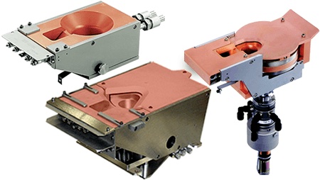
Semiconductor PVD systems use electron beam evaporation sources with precision-machined crucibles and target materials. Pathlink manufactures these for both standard and custom configurations, suitable for metals, alloys, and compound targets used in semiconductor metallisation.
Can sensors be customised for cleanroom environments?
Yes. All Pathlink sensors can be specified for cleanroom compatibility including appropriate materials, connectors, and sealing to prevent contamination. We work from your environment specifications to ensure suitability.
Discuss your semiconductor application.
Tell us your process requirements and we will recommend the right sensor, component, or thermal solution for your fab environment.
Contact Our Engineering Team